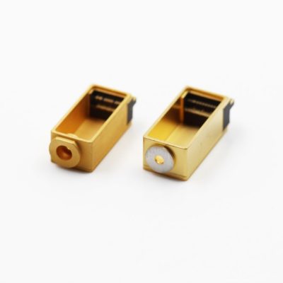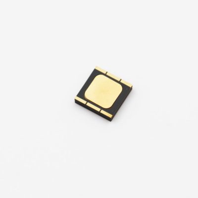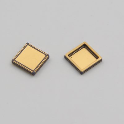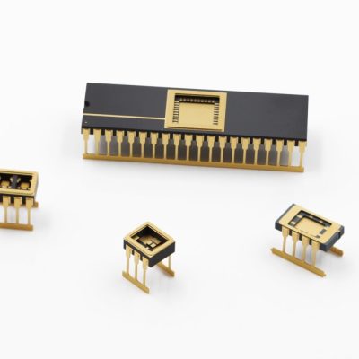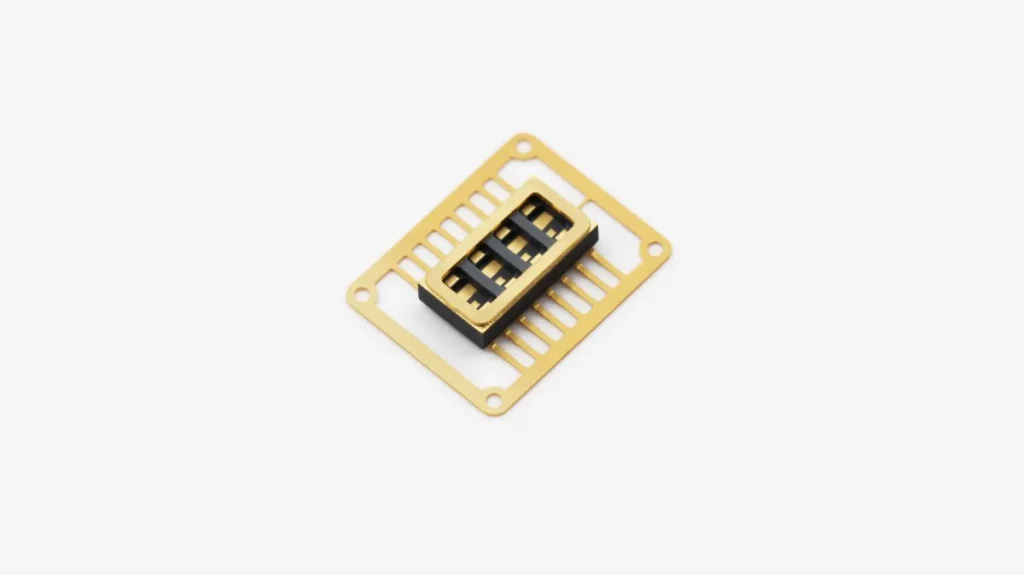
Engineered for miniaturized electronic assemblies, our High-Reliability Ceramic Small Outline IC Packages deliver an exceptional hermetic sealing solution. These advanced ceramic housings are specifically designed to provide unmatched thermal stability, superior electrical conductivity, and robust mechanical strength. By leveraging cutting-edge ceramic manufacturing and precise metallization processes, InSealing provides secure, stable interconnects perfectly suited for integrated circuits functioning in extreme and demanding environments.
When evaluated against standard plastic alternatives, our ceramic small outline packages stand out due to their exceptional hermetic properties, minimal thermal expansion mismatch, and superior durability against vibration and physical shock. Featuring a space-saving footprint and flexible wing-style leads, they are highly optimized for high-density printed circuit board (PCB) layouts, significantly minimizing the physical strain on solder connections.
Technical Specifications
| Category | Item | Code | Standard Dimension | Tolerance | Special Dimension | Tolerance |
| External Structure | Length | L | 5~75 | ±1% | 2~100 | ±0.6% |
| Width | W | 5~75 | ±1% | 2~100 | ±0.6% | |
| Thickness | H | 0.8~4.0 | ±3% | 0.4~5.0 | ±2% | |
| Single-layer Thickness | h | 0.12, 0.15, 0.20, 0.25 | ±0.02 | 0.1 | ±0.01 | |
| Internal Structure | Hole Diameter | Φp1 | 0.13, 0.17, 0.20, 0.25, 0.30, 0.34, 0.42 | ±0.01 | 0.08, 0.10 | ±0.01 |
| Hole Spacing | s1 | 3Φp1 min | – | – | – | |
| Distance from Hole to Edge | s2 | 3Φp1 min | – | – | – | |
| Pad | Φp2 | Φp1+0.1 | – | Φp1+0.05 | – | |
| Side Hole | R | 0.17, 0.21, 0.25, 0.30 | – | Customized Requirements | – | |
| Hole Spacing | s3 | 3R min | – | – | – | |
| Via Position Deviation | s4 | – | ±0.02 | – | ±0.015 | |
| Metallization | Line Width | A | 0.08 min | ±20% | 0.05 min | ±10% |
| Line Width | >0.10 | ±0.02 | >0.10 | ±0.01 | ||
| Line Spacing | B | 0.08 min | ±20% | 0.05 min | ±0.01 | |
| Line Spacing | >0.10 | ±0.02 | – | – | ||
| Distance from Pattern to Edge | C | 0.20 min | – | 0.00 | – |
Key Advantages & Features
- Ultra-compact footprint equipped with stress-relieving wing-style leads
- Outstanding resilience against physical shock and severe continuous vibrations
- Precision dimensional tolerances paired with highly reliable metallization
- Optimized for seamless integration into complex, high-density PCB designs
- Versatile lead pitch options available (e.g., 0.80 mm, 1.00 mm, 1.27 mm)
Primary Applications
- Hermetic housing for a wide array of integrated circuits (ICs)
- Critical and highly dependable electronic assemblies
- Military, aviation, and aerospace electronic systems
- Automation and industrial control machinery
- Advanced medical devices and highly precise analytical instruments
Standard Configurations
| Model Number | Lead Count | Lead Pitch (mm) | Cavity Dimensions (mm) | Outer Dimensions (mm) | Sealing Method |
| CSOP04-01 | 4 | 2.54 | 2.60 * 2.30 | 5.40 * 4.00 | Flat Sealing |
| CSOP08-02 | 8 | 1.27 | 2.74 * 3.00 | 5.00 * 4.40 | |
| CSOP14-03 | 14 | 1.27 | 4.50 * 2.40 | 9.00 * 6.00 | |
| CSOP16-02 | 16 | 1.27 | 1.60 * 2.20 | 10.50 * 5.40 | |
| CSOP16D | 16 | 1.27 | 5.00 * 3.00 | 10.50 * 7.50 | |
| CSOP20-01 | 20 | 1.27 | 6.00 * 4.00 | 12.70 * 7.50 | |
| CSOP20-02 | 20 | 0.65 | 2.80 * 2.80 | 6.60 * 5.50 | |
| CSOP24-03H | 24 | 0.65 | 4.60 * 2.00 | 8.60 * 6.30 | |
| CSOP32-02 | 32 | 1.27 | 12.00 * 9.70 | 20.47 * 12.70 | |
| CSOP56-01 | 56 | 0.80 | 10.80 * 10.30 | 27.30 * 13.30 |