Ceramic Metallization
Home > Ceramic Metallization
Leave Your Number
Let’s Call You Back

Ceramic Metallization
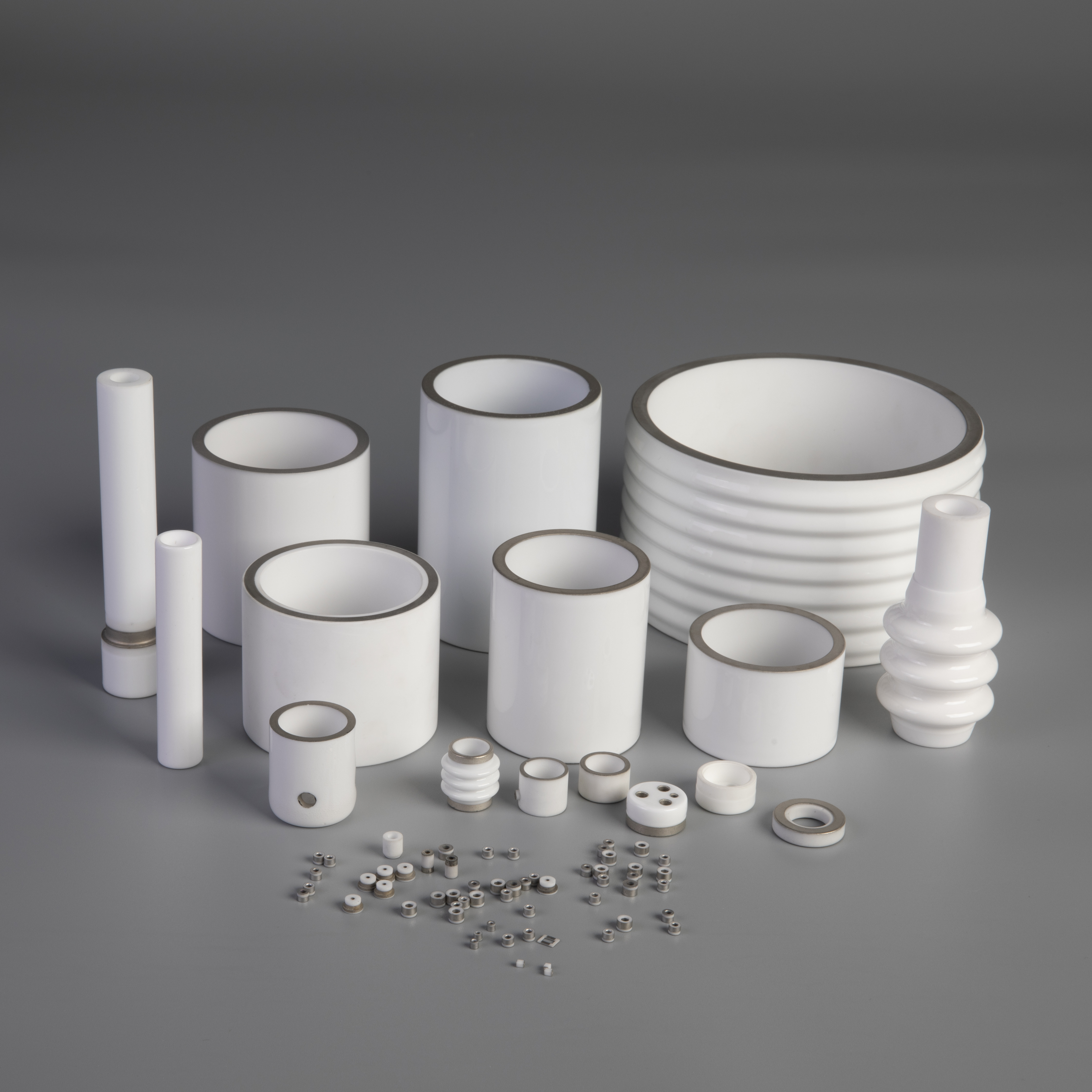
We use thick and thin film technologies in our metallized process, applying proprietary inks and coatings to our ceramics according to individual customer requirements. Whether customers require an electronic circuit path or joining a metal component with ceramic,. We will help you to select the most effective and cost-efficient materials and bonding methods.

-
Refractory Metallized
Using a coating of molybdenum based paints followed by nickel plating, an interface can be provided that enables ceramic/metal assemblies to be formed by brazing providing joints that are hermetically sealed. A layer of molybdenum-manganese is deposited with a typical thickness of 10 to 50 µm after sintering. The metallization sintering process is carefully controlled to achieve a balanced mixture of Molybdenum particles surrounded by a matrix of glass to ensure high bond strength between the metallized layer and the ceramic base.
A range of deposition methods are available depending on the geometry of the component, including:
- Screen printing
- Pad printing
- Brush coating
For cylindrical ceramics, a proprietary automated deposition method delivers consistent uniformity of bandwidth and coating thickness. A thin layer of nickel, typically 2–10 µm, is electrically or chemically deposited on the Molybdenum-Manganese layer to achieve the required wettability for subsequent brazing.
Thick Film Deposition
This involves precious metal pastes, resistors, dielectric insulation layers and sealing glass.
The application of thick film inks provide the engineer with amazing versatility in the use of ceramics. Brushed or screen printed these inks are fired onto the ceramic at 850° providing a secure interface. Inks are supplied in a variety of different materials including gold, silver, copper, glass, dielectric and a range of resistive inks. Nominally 10 microns thick per application, thick film inks can be applied in multi layers to increase coating thickness as required. Gold layers can be wire bonded and silver layers can be soldered.
Typical Applications:
- Instrumentation
- Control systems
- Guidance systems
- IR and UV detectors
- Circuit boards
Thin Film Deposition
In some cases it is necessary to apply a thin metallized layer to ceramic surfaces for discharging or electrical field generation. A range of coatings are available including aluminum, gold and titanium at typically 1-2 microns thick. Virtually any patterns can be applied, and layers are even and consistent. Multi layers of differing materials can be applied such as nickel chrome and nickel gold. This process does allow subsequent electroplating should there be a requirement. Physical vapor deposition, or PVD, is used to apply thin metallization or coating to fully dense ceramic