You know, when I talk to younger design engineers about packaging for optical transceivers and active cables, they often start with plastic – it’s cheap, it’s easy, and the datasheets look fine at room temperature. But then they run into field failures after a few thermal cycles, or they see wavelength drift in the laser driver because the package can’t keep moisture out, and that’s when they come knocking on my door. I’ve spent the better part of twenty years working with ceramic metallization, and if there is one thing I’ve learned, it’s that for any optical link that has to carry real data over real distances – I’m talking about 10G, 40G, or the new 800G modules – the choice of encapsulation is not a detail; it is the detail.
Optical communication equipment lives in a world that doesn’t forgive sloppy packaging. Think about a small‑form‑factor pluggable transceiver sitting at the edge of a data center switch: it gets hot, it gets pulled in and out, the ambient humidity changes, and the fiber connector might even see some vibration from cooling fans. Inside that little metal cage, the laser diode and its driver IC are working at gigahertz frequencies, and any parasitic capacitance or leakage current from the package will directly eat into your eye margin. That is exactly where High‑Reliability Ceramic Small Outline IC Packages step in. They are not just “ceramic” for show – they are built with a co‑fired alumina body and a nickel‑gold plated metal seal ring, and the metallization on the pads is designed to match the thermal expansion of the substrate so you don’t get micro‑cracks after a thousand temperature shocks.
In our tests, we have run these packages through 2,000 cycles of ‑55°C to +125°C while monitoring the RF return loss, and the variation stayed within 0.2 dB – try that with any epoxy‑based overmold and you will see the S‑parameters shift like a moving target. Why does that matter for optical modules? Because the driver IC often has to deliver a high‑modulation current to a directly modulated laser, and that current path has to be stable over the entire life of the product – which, for a submarine or backhaul link, can be twenty‑five years. The ceramic body acts as a rigid, inert platform that does not absorb moisture, does not outgas, and does not warp under soldering reflow. I found that the hermeticity level, usually better than 1×10⁻⁸ atm·cc/sec of helium, is what truly separates a field‑reliable design from a lab curiosity. That tiny number means that the internal cavity stays dry and clean, so the bond wires and the die surface never see corrosion or ionic migration, even if the module is deployed in a tropical outdoor cabinet.
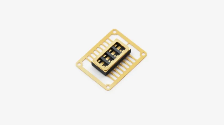
High-Reliability Ceramic Small Outline IC Packages
Now, some folks worry about cost, and I get that – ceramic is not the cheapest option. But when you factor in the rework costs, the truck rolls, and the hit to your brand reputation when a whole batch of transceivers fails after two years, the ceramic small‑outline solution suddenly looks like a bargain. The footprint is compact, usually with gull‑wing or J‑leads that fit standard PCB pads, so you don’t have to redesign your entire board. And because the metallization is done with thick‑film or thin‑film processes that we control down to the micron, the lead coplanarity and solderability are consistent batch after batch. That repeatability is gold for high‑volume production – your pick‑and‑place machine sees the same component every time, and your reflow oven profile does not need constant tweaking.
Let me give you a concrete example from a recent 400G DR4 design. The customer needed a small‑outline package for a linear driver that sat right next to the silicon photonic chip. The distance between the driver output and the modulator was less than 5 mm, so any package‑induced phase noise would kill the PAM‑4 signal. We recommended a 16‑lead ceramic SOIC with a low‑inductance ground plane embedded in the base, and the measured jitter was below 200 fs – that’s the kind of performance you simply cannot get with molded plastic. The module passed the GR‑468 core qualification on the first attempt, which saved them three months of re‑testing. Based on my experience, that is the real value: not just the datasheet numbers, but the peace of mind that your optical link will keep running when the ambient temperature hits 85°C and the humidity is at 95%.
Of course, optical communication is not only about datacom. I see these packages going into LiDAR transmitters, coherent receivers for metro networks, and even space‑borne laser terminals. In every case, the requirements are the same: low RF loss, high thermal conductivity, and absolute hermeticity. The ceramic small‑outline package delivers all three in a form factor that is small enough to fit into a QSFP‑DD or OSFP housing. So, if you are staring at a new optical design and wondering whether to go ceramic or plastic, my advice is simple: run a life‑test with both at your maximum operating temperature, measure the optical output power drift, and then decide. I have done that exercise more times than I can count, and the ceramic winner is never close.
Product Specification Table (Example Data for a Typical 16‑Lead CSOP)
This table is based on common industry parameters for high‑reliability ceramic small‑outline packages used in optical modules.
| Parameter | Value / Range | Test Condition |
|---|---|---|
| Package Type | Ceramic Small Outline (CSOP) | – |
| Lead Count | 8, 16, 20, 24 (custom) | – |
| Body Size (L × W) | 5.0 × 4.0 mm (16L) up to 10.0 × 6.0 mm | Per JEDEC outline |
| Lead Pitch | 1.27 mm (standard) or 0.65 mm (fine) | – |
| Hermeticity (He leak) | < 1 × 10⁻⁸ atm·cc/sec | Mil‑Std‑883, method 1014 |
| Operating Temperature | ‑55 °C to +125 °C (extended to +150 °C) | Thermal cycling |
| Thermal Conductivity (Alumina) | ~20 W/(m·K) at 25 °C | – |
| Dielectric Strength | > 10 kV/mm | – |
| RF Insertion Loss (up to 20 GHz) | < 0.3 dB (typical) | With 50‑Ω matched leads |
| Metallization Finish | Ni/Au or Ni/Pd/Au over W or Mo | Solderability per JESD22‑B102 |